The building blocks of any electronic circuit or chip are resistor,capacitor and inductor . The most surprising and astonishing thing regarding these are the contrast between their size and their capabilities(functions).
Many felt about a decade ago that electronic components have reached their smallest size but they were totally wrong.If they had seen today’s electronics industry they would surely take back their word.While handling electronic components like transistor,resistor,etc., they would often slip from between our fingers.We would of course get cross with them but one would surely marvel once they know it’s capabilities. I am one among them.
Electronics industry is mutating and developing from past a set of decades.This is mainly due to R&D being carried out and also due to increase in electronics market today.It is totally due to awareness in public.
The main increase in electronic goods is due to its features like, compactness,small size and flashy fabrications. Let’s concentrate on their size and compactness.They are key features of any electronic goods.
To make this feature even more strong ,rigorous R&D has been carried on it and this has yielded good.The technology used to improve compactness and decrease the size of a circuit has been constantly changing .
Process of development:
SSI (small-scale integration)
MSI (medium-scale integration)
LSI (LARGE-SCALE INTEGRATION)
VLSI (very large-scale integration)
WSI (WAFER-SCALE INTEGRATION)
SOC (system-on-a-chip)
3D-IC (three-dimensional integrated circuit)
SMT (Surface Mounted Technology)
Let’s deal with the latest SMT technology.
Surface-mount technology (SMT) is a method for making electronic circuits in which the components are mounted or placed directly onto the surface of printed circuit boards (PCBs). An electronic device so made is called a surface-mount device (SMD). In the industry it has largely replaced the through-hole technology
Through-hole technology is nothing but construction method of fitting components with wire leads into holes in the circuit board.
Both technologies can be used on the same board for components not suited to surface mounting such as transformers and heat-sinked power semiconductors.
An SMT component is usually smaller than its through-hole counterpart because it has either smaller leads or no leads at all. It may have short pins or leads of various styles, flat contacts, a matrix of solder balls (BGAs), or terminations on the body of the component. Actually components were mechanically redesigned to have small metal tabs or end caps that could be directly soldered to the surface of the PCB. Components became much smaller and component placement on both sides of a board became far more common with surface mounting than through-hole mounting, allowing much higher circuit densities.
Much of the pioneering work in this technology was by IBM,introduced in 1960 in a small-scale computer was later applied in the Launch Vehicle Digital Computer used in the Instrument Unit that guided all Saturn IB and Saturn V vehicles.
Components became much smaller and component placement on both sides of a board became far more common with surface mounting than through-hole mounting, allowing much higher circuit densities. Often only the solder joints hold the parts to the board, although parts on the bottom or “second” side of the board may be secured with a dot of adhesive to keep components from dropping off inside reflow ovens if the part has a large size or weight. Adhesive is also used to hold SMT components on the bottom side of a board if a wave soldering process is used to solder both SMT and through-hole components simultaneously. Alternatively, SMT and throughhole components can be soldered together without adhesive if the SMT parts are first reflow-soldered, then a selective solder mask is used to prevent the solder holding the parts in place from reflowing and the parts floating away during wave soldering. Surface mounting lends itself well to a high degree of automation, reducing labor cost and greatly increasing production rates. SMDs can be one quarter to one-tenth the size and weight, and one-half to one-quarter the cost of equivalent through-hole parts.
Understanding it’s size.
Isn’t it really worthy to learn in detail?
How do they do this wonder?
Assembly Work:
Where components are to be placed, the printed circuit board normally has flat, usually tin-lead, silver, or gold plated copper pads without holes, called solder pads. Solder paste, a sticky mixture of flux and tiny solder particles, is first applied to all the solder pads with a stainless steel or nickel stencil using a screen printing process. It can also be applied by a jet-printing mechanism, similar to aninkjet printer. After pasting, the boards then proceed to the pick-and-place machines, where they are placed on a conveyor belt. The components to be placed on the boards are usually delivered to the production line in either paper/plastic tapes wound on reels or plastic tubes. Some large integrated circuits are delivered in static-free trays.
Numerical control pick-and-place machines remove the parts from the tapes, tubes or trays and place them on the PCB. The boards are then conveyed into the reflow soldering oven. They first enter a pre-heat zone, where the temperature of the board and all the components is gradually, uniformly raised. The boards then enter a zone where the temperature is high enough to melt the solder particles in the solder paste, bonding the component leads to the pads on the circuit board. The surface tension of the molten solder helps keep the components in place, and if the solder pad geometries are correctly designed, surface tension automatically aligns the components on their pads. There are a number of techniques for reflowing solder.
One is to use infrared lamps; this is called infrared reflow. Another is to use a hot gas convection. Another technology which is becoming popular again is special fluorocarbon liquids with high boiling points which use a method called vapor phase reflow. Due to environmental concerns, this method was falling out of favor until lead-free legislation was introduced which requires tighter controls on soldering. Currently, at the end of 2008, convection soldering is the most popular reflow technology using either standard air or nitrogen gas. Each method has its advantages and disadvantages. With infrared reflow, the board designer must lay the board out so that short components don’t fall into the shadows of tall components.
Component location is less restricted if the designer knows that vapor phase reflow or convection soldering will be used in production. Following reflow soldering, certain irregular or heat-sensitive components may be installed and soldered by hand, or in large-scale automation, by focused infrared beam (FIB) or localized convection equipment. If the circuit board is double-sided then this printing, placement, reflow process may be repeated using either solder paste or glue to hold the components in place. If a wave soldering process is used, then the parts must be glued to the board prior to processing to prevent them from floating off when the solder paste holding them in place is melted.
After soldering, the boards may be washed to remove flux residues and any stray solder balls that could short out closely spaced component leads. Rosin flux is removed with fluorocarbon solvents, high flash point hydrocarbon solvents, or low flash solvents e.g. limonene (derived from orange peels) which require extra rinsing or drying cycles. Water soluble fluxes are removed with deionized water and detergent, followed by an air blast to quickly remove residual water. However, most electronic assemblies are made using a “No-Clean” process where the flux residues are designed to be left on the circuit board [benign]. This saves the cost of cleaning, speeds up the manufacturing process, and reduces waste.
The major technical considerations for implementing SMT include Surface mount land pattern design, PB design for manufacturability, solder paste printing, component placement, reflow soldering, wave soldering, cleaning, and repair/rework. These areas must be studied and thoroughly understood to achieve high quality, reliable surface mount products. For more details on board assembly processing. Surface Mount Technology is latest PCB designing technique which has which has high efficiency & it is widely used in industrial production due to steadiness in its production. It further has scope for its betterment in area of reducing the soldering work i.e use of soldering material as because of this the efficiency in space management.
The added advantage of this technology is:
Rework:
Defective surface-mount components can be repaired by using soldering irons (for some connections), or using a non-contact rework system. In most cases a rework system is the better choice because SMD work with a soldering iron requires considerable skill, and is not always feasible. There are essentially two non-contact soldering/ desoldering methods: infrared soldering and soldering with hot gas.
Infrared:
With infrared soldering, the energy for heating up the solder joint is transmitted by long- or short-wave infrared electromagnetic radiation.
Benefits:
- Easy setup
- No compressed air required
- No requirement for different nozzles for many component shapes and sizes, reducing cost and the need to change nozzles
- Fast reaction of infrared source (depends on system used)
Disadvantages:
- Central areas will be heated more than peripheral areas
- Temperature control is less precise, and there may be peaks
- Nearby components must be shielded from heat to prevent damage, which requires additional time for every board
- Surface temperature depends on the component’s albedo: dark surfaces will be heated more than lighter surfaces
- The temperature additionally depends on the surface shape. Convective loss of energy will reduce the temperature of the component
- No reflow atmosphere possible
Hot air:
During hot gas soldering, the energy for heating up the solder joint is transmitted by a hot gas. This can be air or inert gas (nitrogen).
Benefits:
- Simulating reflow oven atmosphere
- Some systems allow switching between hot air and nitrogen
- Standard and component-specific nozzles allow high reliability and faster processing
- Allow reproducible soldering profiles
- Efficient heating, large amounts of heat can be transferred
- Even heating of the affected board area
- Temperature of the component will never exceed the adjusted gas temperature
- Rapid cooling after reflow, resulting in small-grained solder joints (depends on system used)
Disadvantages:
- Thermal capacity of the heat generator results in slow reaction whereby thermal profiles can be distorted (depends on system used)
Reworking usually corrects some type of error, either human- or machine-generated, and includes the following steps:
- Melt solder and remove component (s)
- Remove residual solder
- Print solder paste on PCB, directly or by dispensing
- Place new component and reflow.
Sometimes hundreds or thousands of the same part need to be repaired. Such errors, if due to assembly, are often caught during the process. However, a whole new level of rework arises when component failure is discovered too late, and perhaps unnoticed until the end user of the device being manufactured experiences it. Rework can also be used if products of sufficient value to justify it require revision or re-engineering, perhaps to change a single firmware-based component. Reworking in large volume requires an operation designed for that purpose.
Having understood then in detail,now let us see how to recognize(decode) the components:
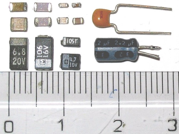
Resistors:
For 5% precision SMD resistors usually are marked with their resistance values using three digits, two significant digits and a multiplier digit. These are quite often white lettering on a black background, but other colored backgrounds and lettering can be used.
The black or colored coating is usually only on one face of the device, the sides and other face simply being the uncoated, usually white ceramic substrate. The coated surface, with the resistive element beneath is normally positioned face up when the device is soldered to the board although they can rarely be seen mounted with the uncoated underside face up, whereby the resistance value code is not visible.
For 1% precision SMD resistors, the EIA-96 code is used, as three digits would otherwise not convey enough information. This code consists of two digits and a letter: the digits denote the value’s position in the E96 sequence, while the letter indicates the multiplier.
- Typical examples of resistance codes
- 102 = 10 00 = 1,000 Ω = 1 kΩ
- 0R2 = 0.2 Ω
- 684 = 68 0000 = 680,000 Ω = 680 kΩ
- 68X = 499 × 0.1 = 49.9 Ω
There is an online tool to translate codes to resistance values on some websites. resistors can be found in several types of material but the most common is ceramic resistor where the substrate is ceramic. value are available in several tolerances defined in EIA Decade Values Table :
E3 50% tolerance (no longer used)
E6 20% tolerance (now seldom used)
E12 10% tolerance
E24 5% tolerance
E48 2% tolerance
E96 1% tolerance
E192 0.5, 0.25, 0.1% and higher tolerances
Capacitors:
Non electrolytic capacitors are usually unmarked and the only reliable method of determining their value is removal from the circuit and subsequent measurement with a capacitance meter or impedance bridge. The materials used to fabricate the capacitors, such as Nickel Tantalate, possess different colours and these can give an approximate idea of the capacitance of the component.
- Light grey body colour indicates a capacitance which is generally less than 100 pF.
- Medium Grey colour indicates a capacitance anywhere from 10 pF to 10 nF.
- Light brown colour indicates a capacitance in a range from 1 nF to 100 nF.
- Medium brown colour indicates a capacitance in a range from 10 nF to 1 μF.
- Dark brown colour indicates a capacitance from 100 nF to 10 μF.
- Dark grey colour indicates a capacitance in the μF range, generally 0.5 to 50 μF, or the device may be an inductor and the dark grey is the color of the ferrite bead. (An inductor will measure a low resistance to a multimeter on the resistance range whereas a capacitor, out of the circuit, will measure a near infinite resistance.)
Generally physical size is proportional to capacitance and voltage^2 for the same dielectric. For example, a 100 nF 50 V capacitor may come in the same package as a 10 nF 150 V device.
SMD (non electrolytic) capacitors, which are usually monolithic ceramic capacitors, exhibit the same body color on all four faces not covered by the end caps.
SMD electrolytic capacitors, usually tantalum capacitors, and film capacitors are marked like resistors, with two significant figures and a multiplier in units of pico Farads or pF, (10−12 Farad.)
- Examples
- 104 = 100 nF = 100,000 pF
- 226 = 22 μF = 22,000,000 pF
The electrolytic capacitors are usually encapsulated in black or beige epoxy resin with flat metal connecting strips bent underneath. Some film or tantalum electrolytic types are unmarked and possess red, orange or blue body colors with complete end caps, not metal strips.
Inductors:
Due to the small dimensions of SMDs, SMT inductors are limited to values of less than about 10 mH. Smaller inductance with moderately high current ratings are usually of the ferrite bead type. They are simply a metal conductor looped through a ferrite bead and almost the same as their through-hole versions but possess SMD end caps rather than leads. They appear dark grey and are magnetic, unlike capacitors with a similar dark grey appearance. These ferrite bead type are limited to small values in the nH (nano Henry), range and are often used as power supply rail decouplers or in high frequency parts of a circuit. Larger inductors and transformers may of course be through-hole mounted on the same board.
SMT inductors with larger inductance values often have turns of wire or flat strap around the body or embedded in clear epoxy, allowing the wire or strap to be seen. Sometimes a ferrite core is present also. These higher inductance types are often limited to small current ratings, although some of the flat strap types can handle a few amps.
As with capacitors, component values and identifiers are not usually marked on the component itself; if not documented or printed on the PCB, measurement, usually removed from the circuit, is the only way of determining them.
Discrete semiconductors:
Discrete semiconductors, such as transistors, diodes and F.E.T.s are often marked with a two- or three-symbol code in which the same code marked on different packages or on devices made by different manufacturers can translate to different devices.
Many of these codes, used because the devices are too small to be marked with more traditional numbers used on through-hole equivalent devices, correlate to more familiar traditional part numbers when a correlation list is consulted.
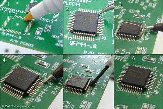
Some pictures that can make you understand SMT technology better: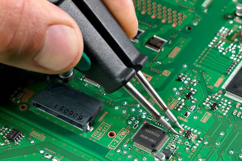
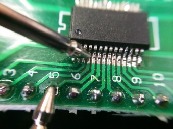
Overall process of SMT:
Finally,
Advantages :
The main advantages of SMT over the older through-hole technique are:
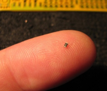
- Smaller components. As of 2012 smallest was 0.4 × 0.2 mm (0.016 × 0.008 in: 01005). Expected to sample in 2013 are 0.25 × 0.125 mm .
- Much higher component density .
- Lower initial cost and time of setting up for production.
- Fewer holes need to be drilled.
- Simpler and faster automated assembly. Some placement machines are capable of placing more than 136,000 components per hour.
- Small errors in component placement are corrected automatically as the surface tension of molten solder pulls components into alignment with solder pads.
- Components can be placed on both sides of the circuit board.
- Lower resistance and inductance at the connection; consequently, fewer unwanted RF signal effects and better and more predictable high-frequency performance.
- Better mechanical performance under shake and vibration conditions.
- Many SMT parts cost less than equivalent through-hole parts.
- Better EMC compatibility (lower radiated emissions) due to the smaller radiation loop area .
Disadvantages :
- Manual prototype assembly or component-level repair is more difficult and requires skilled operators and more expensive tools, due to the small sizes and lead spacings of many SMDs.
- SMDs cannot be used directly with plug-in breadboards .
- SMDs’ solder connections may be damaged by potting compounds going through thermal cycling.
- Solder joint dimensions in SMT quickly become much smaller as advances are made toward ultra-fine pitch technology. The reliability of solder joints becomes more of a concern, as less and less solder is allowed for each joint. Voiding is a fault commonly associated with solder joints, especially when reflowing a solder paste in the SMT application. The presence of voids can deteriorate the joint strength and eventually lead to joint failure.
- SMT is unsuitable for large, high-power, or high-voltage parts, for example in power circuitry. It is common to combine SMT and through-hole construction, with transformers, heat-sinked power semiconductors, physically large capacitors, fuses, connectors, and so on mounted on one side of the PCB through holes.
- SMT is unsuitable as the sole attachment method for components that are subject to frequent mechanical stress, such as connectors that are used to interface with external devices that are frequently attached and detached.